Introduction
In this world of modern engineering, every device has an electronic circuit that makes it more advanced and compact. There is one thing that is called the heart of any electronic circuit which is an Integrated Circuit or ICs (It can be a microprocessor, FPGA, or any normal GATE IC). The latest technology behind the designing of these ICs is the most complex and critical part of electronics. VLSI design is the process that is used to design these Integrated Circuits.
 |
| VLSI Design Flow- A Complete Overview of the VLSI Design Flow Chart |
So are you looking for information on this complex technology? So you are at the right place. In this article, we will provide a comprehensive overview of the VLSI Design Flow.
VLSI Design Flow Includes
- System Specification
- Architectural Design
- Functional and Logic Design
- Circuit Design
- Physical Design
- Physical Verification
- Fabrication
- Packaging and Testing
Before proceeding please read this prerequisite post first-
Table of Contents
VLSI Design Flow
VLSI (Very Large Scale Integration) Design Flow is the process of designing and developing an integrated circuit (IC) or a microchip. It involves a series of steps that includes designing, fabrication, testing, and packaging of the IC. The VLSI Design Flow is a crucial process, as it determines the performance, reliability, and cost-effectiveness of the IC.
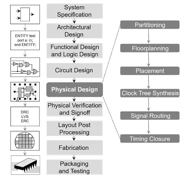 |
| VLSI Design Flow Chart (image credit-wikipedia.org) |
Explanation of the VLSI Design Flow Chart is as follows:-
1. System Specification:
This is the first step of the VLSI design which involves defining the overall goals and requirements of the system. These goals are decided by Chip Architects, circuit Designers, Product Marketers, Production Managers, and Layout and Library designers. These goals include functionality, performance, physical dimensions, and production technology of the system.
The system specification stage is crucial as it sets the foundation for the entire design process. The system specifications are used to create a design plan that outlines the different stages of the design process and the requirements for each stage. The plan also includes timelines and deadlines for each stage to ensure that the project stays on track.
2. Architectural Design:
As the name, this step decides the overall architecture of the IC to meet the goals set in the first system specification step. It includes deciding the blocks of IC line analog and mix signal block, Memory management, deciding no of cores, digital signal processors (DSPs), internal-external communications, standard protocols like CAN, UART, I2C, etc, pinout and packages like BGA, PGA, etc.
The architectural design stage is crucial as it ensures that the chip or system is designed to meet the required specifications. The architectural design stage involves a lot of brainstorming and analysis to come up with the most optimal architecture for the chip or system.
3. Functional and Logic Design:
Once the architecture is defined the connectivity and functionality can be defined in this step. That is each module has an input-output and timing behavior. Logic design is performed at the register transfer level (RTL) using a hardware description Language (HDL) eg the software programs that define the functional and timing behavior of a chip. The two most common HDL are used Verilog and VHDL. HDL modules are then simulated and verified.
There are logic synthesis tools that automate the process of converting HDL into low-level circuit elements. That is by using Verilog or VHDL description and the technology library a logic synthesis tool can map all the functionalities to the list of signal nets, and specific circuit elements like transistors.
4. Circuit Design:
After the automatic conversion of standard cells or higher, there are several critical and low-level elements that must be designed at the transistor level this is called circuit design.
The circuit design phase is where the RTL description is translated into a circuit-level implementation. This involves the creation of a gate-level netlist, which is a low-level description of the circuit in terms of logic gates.
The gate-level netlist is then optimized to improve performance, power consumption, and area utilization. This optimization is done using computer-aided design (CAD) tools, which are software programs that automate the design process.
The gate-level netlist is also verified through simulation to ensure that it functions correctly. This involves the creation of test benches, which are software programs that generate inputs to the circuit and verify that the outputs are correct.
For example, elements like RAM blocks, I/O, analog circuits, Multipliers, and ESD protection circuits are designed in circuit-level design. The verification of circuit design is done by the simulation tools like SPICE.
5. Physical Design:
In physical design, all components like macros, cells, gates, transistors, etc with fixed sizes and shapes are placed at the location in the fabrication layer to perform appropriate routing. Physical design is performed according to DRC (Design Rule Check) which depends on the capabilities of fabrication technology. For example, wires must be kept at a proper distance between them. Physical design directly impacts circuit performance, area, reliability, power, and manufacturing yield.
Due to the high complexity of physical design, it split into several steps as follows-
1) Partitioning
2) Floorplanning
3) Power and Ground Routing
4) Placement
5) Clock Network Synthesis
6) Global Routing
7)Detailed Routing
8) Timing Closure
The physical design phase is a critical step in the VLSI design flow because the physical layout can have a significant impact on the performance, power consumption, and area utilization of the chip. Therefore, the physical design is optimized using CAD tools to improve these metrics.
6. Physical Verification:
After the physical design, the designed layout must be verified to ensure correct functionality. In this step after verification, some problems found can be neglected if they cause a nominal impact on performance but if causing a major impact then the layout needs to be changed. This is done by experienced design engineers. Some types of verifications are performed in this step as follows-
1) Design Rule Check (DRC)
2) Layout vs Schmatic(LVS)
3) Parasitic Extraction
4) Antenna Rule Checking
5) Electrical Rule Checking (ERC)
7. Fabrication:
The final Layout represented in the GDSII stream format is sent for manufacturing at a dedicated silicon foundry(Fab). The handoff of the design to the manufacturing process is called tape out. The generation of data for manufacturing is sometimes referred to as streaming out. At fab, the design pattern is printed on different layers using photolithography. ICs are manufactured on round silicon wafers of diameter from 200mm to 300mm. The IC must be tested after fabrication and cut into smaller pieces to get the end chip.
The fabrication process is a complex and expensive process that requires specialized equipment and facilities. Therefore, it is typically outsourced to semiconductor foundries that specialize in chip manufacturing.
8. Packaging and Testing:
After dicing chips are packaged according to the design process. Chip package types like dual in-line packages (DIPs), pin grid arrays (PGAs), and ball grid arrays (BGA). After the chip is placed in the die cavity the pins are connected to the pins of the package and then it is sealed.
The testing phase is a critical step in the VLSI design flow because it ensures that the final product meets the design specifications and is free from defects. Therefore, the testing process is performed rigorously to ensure the quality of the final product.
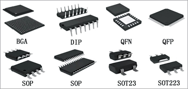 |
| IC Packages (img credit- Electronics for you) |
Conclusion
The VLSI design flow is a complex process that involves various steps, starting from system specification to packaging and testing. Each step plays a vital role in the overall design process, and any error or issue at any stage can lead to significant problems in the final product.
Therefore, The VLSI design is a complex process that has many steps involved, each of which is critical for the successful design and production/manufacturing/fabrication of an integrated circuit. Designers can create efficient and reliable ICs that meet the desired performance requirements with minimum power consumption and less area by following this process.
Overall, the VLSI design flow is an essential process that plays a significant role in the development of modern electronic devices, and a thorough understanding of the various steps involved can help designers create efficient and reliable products that meet the demands of modern consumers.
What is VLSI design flow?
The VLSI (Very Large Scale Integration) design flow is the process of designing complex IC (Integrated Circuits) like microprocessors, FPGA, etc from start to finish.
What are the steps involved in the VLSI design flow?
System Specification-Architectural Design-Functional and Logic Design-Circuit Design-Physical Design-Physical Verification-Fabrication-Packaging and Testing
What is the physical design and what are its different types in VLSI design flow?
In physical design, all components like macros, cells, gates, transistors, etc with fixed sizes and shapes are placed at the location in the fabrication layer to perform appropriate routing.
1) Partitioning
2) Floorplanning
3) Power and Ground Routing
4) Placement
5) Clock Network Synthesis
6) Global Routing
7)Detailed Routing
8) Timing Closure
What is tape out?
The handoff of the design to the manufacturing process is called tapeout.


Discover cutting-edge advancements in VLSI design that electronics students should be aware of for future opportunities. To read the full blog Click here Thank You.
ReplyDelete